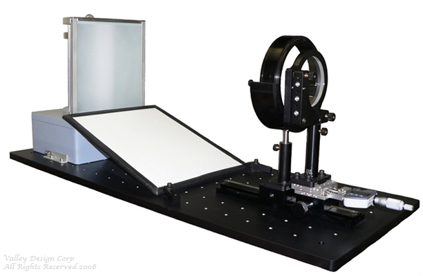
Optical interferometer for thin wafers
Introducing the New Indars Optical Interferometer
Specially designed to measure thin, transparent wafers and substrates
From Necessity to Invention
- Valley Design is not an equipment manufacturer – We lap and polish optical, electro-optical and semiconductor materials
- Valley specializes in ultra-thin < 500um substrates and wafers
- Customers’ specifications for reflective flatness or surface figure range from 1/4 band (1/8 λ) to 1-2 bands/inch
- We could find no accurate way to measure the flatness of these thin, transparent wafers due to the limitations of traditional methods.
Fizeau Laser Interferometer
- Only measures wavefront distortion, but not reflective flatness from a single side of a transparent wafer.
- When an opaque film is applied to one side, this distorts the flatness of a thin wafer, providing inaccurate readings.
- Fizeau phase shifting instruments which claim to measure reflective flatness, are very expensive.
Optical Flats
- An optical flat is placed in direct contact with the wafer to be measured, causing scratches in both.
- When thin wafers are placed either on top or beneath the optical flat, thin parts can conform to the surface
shape of the optical flat, or be flattened by the optical flat, causing inaccurate readings.
- Traditional optical flat readings are performed horizontally, which introduce bending components caused
by gravitational force.
What is needed for an accurate flatness reading?
- Wafers need to be held vertically to eliminate the effects of gravity
- Wafers need to be measured without the application of flatness distorting opaque films
- Wafers need to reference an optical flat, without any direct contact.
Benefits of the new Indars Interferometer
- The Indars Interferometer has been patented and is optimized to measure thin, transparent wafers, and
can currently measure up to 300mm diameter. Larger diameters are available, and are limited only by the
availability of larger optical flats.
- The new scheme allows for vertical placement of the sample under test. An optical flat is referenced,
but not directly contacted.
- The need for distorting opaque films has been eliminated.
- Versatile, lower cost solution to provide accurate flatness readings.